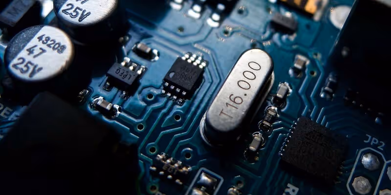
Fuel innovation in semiconductor manufacturing and design. Companies in the U.S. semiconductor industry—covering wafer fabrication, chip design, packaging, process engineering—are engaged in high‑tech research and development. Many of these activities qualify for the federal R&D Tax Credit under IRC §41, as well as state‑level incentives.

Examples of qualifying activities in semiconductor manufacturing & design
- Node / Process Development Testing and refining new process nodes (e.g., 3nm, 2nm), novel etch or deposition techniques, defect‑density reduction, yield improvement.
- Advanced Packaging & Integration Developing heterogeneous integration, 3D‑stacked dies, chip‑let architectures, new substrate materials or interconnect strategies.
- Materials & Photo‑Lithography Innovation Examining new resist materials, EUV/XUV lithography enhancements, new materials for interconnects, diffusion/implant trials.
- Design & Simulation of Chip Architectures Using CAD/EDA tools, simulation of new logic, memory or analog‑mixed signal architectures, modelling power and performance trade‑offs.
- Automation, Data Analytics & Yield Engineering Implementing AI‑based defect‑detection systems, automated inspection, high‑throughput measurement and test systems.
What qualifies as R&D in Semiconductors?

To qualify, activities must:
- Pursue a permitted purpose such as developing a new node process, advanced packaging technique, defect‑reduction technology, or next‑generation chip architecture
- Address technical uncertainty about method, capability, or design in micro‑electronics, materials science, photolithography, process engineering
- Follow a process of experimentation through wafer‑trial runs, lithography studies, defect tracking experiments, or packaging validation
- Be technological in nature, grounded in electrical engineering, materials engineering, chemical engineering or software modelling of chip behavior
Qualified Research Expenses (QREs)
Roles commonly involved in qualifying activities
- Semiconductor process engineers (fab, front‑end/back‑end)
- Chip design engineers (logic, memory, analog, mixed‑signal)
- Materials scientists and lithography specialists
- Automation engineers for metrology, inspection, yield improvement
- External research partners, foundries, lab facilities
What does not qualify
- Routine wafer production or chip manufacturing without experimental change
- Maintenance, scale‑up of known processes without uncertainty
- General administrative, sales or marketing functions
- Equipment purchases for standard production not directly tied to R&D
Compliance and Documentation
Following the One Big Beautiful Bill Act (OBBBA) signed July 4, 2025, §174 now allows immediate expensing of domestic research expenses for tax years beginning on or after January 1, 2025. Taxpayers may also elect optional amortization under new §174A. Foreign research expenses must still be amortized over 15 years. This is separate from the §41 credit but impacts overall tax planning.
- Project goals (e.g., new node yield targets), test plans, manufacturing trial logs
- Wafer‑trial results, defect counts, yield improvement data, material trial outcomes
- Simulation logs, design revisions, packaging test data
- Employee hours, role descriptions, test vs production differentiation
- Audit‑ready demonstration of the four‑part test
Frequently Asked Questions
Yes — if they are engaging in process innovation, materials research, design optimisation, packaging enhancement or automation of fab/test flows.
Wages for engineers and scientists, supplies (wafer lots, masks, material samples), software modelling tools, and contract research in labs or foundries.
Wafer fabrication plants, design houses, packaging/test facilities, materials suppliers, and yield‑improvement labs—provided they are conducting research, not just production.
Routine manufacturing, production scaling of established processes, purely administrative functions, standard equipment purchases.
Savings depend on the scale and scope of the R&D—but companies can claim a significant portion of qualified research expenses if properly documented and supported.
Keep detailed records of trial lots, defect statistics, simulation results, design iterations, material evaluations, tool time, and employee time tied to R&D tasks.
Next Steps

Use our calculator to estimate your potential federal and state benefits

Schedule a consultation to structure your row crop research activities
If you are innovating in agriculture, you may already be doing R&D. Let's make sure you are rewarded for it.
Contact Strike Tax Advisory
Ready to maximize your R&D tax credits? Get in touch with our team of experts.

How much could I get back for
Semiconductors
?